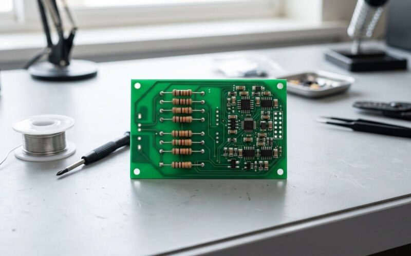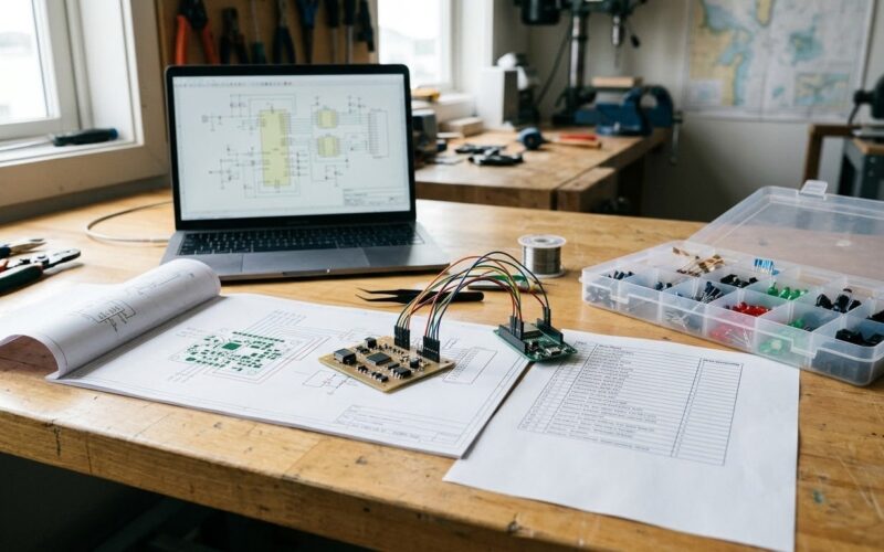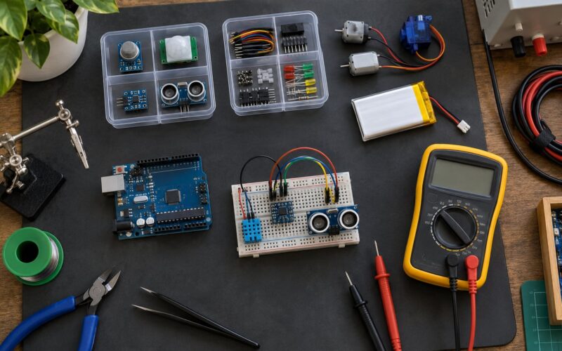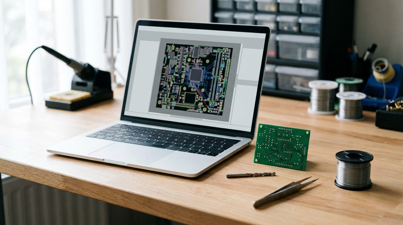
How are PCBs made? By transferring a circuit design onto a copper-clad board, removing the copper that is not part of the circuit, drilling and plating the connections between layers, then adding solder mask, a surface finish and silkscreen before the components go on. Most fabrication runs through four phases: design, imaging and etching, layering and drilling, and masking, finishing and testing.
I have built boards for ocean-drifting sensor pods and small sailing robots, and the part that still surprises people is how little of the process is glamorous. A bare board is glass, resin and copper foil until a machine burns an image into it and chemistry takes everything else away.
Table of Contents
- How Are PCBs Made? The Complete Manufacturing Process
- What Is a PCB and Why Is Manufacturing Important?
- How Are PCBs Made From a Schematic?
- How Are PCBs Made Using Different Manufacturing Methods?
- What Happens During PCB Fabrication?
- 1. CAM review and panelization
- 2. Material preparation and cutting
- 3. Imaging the artwork
- 4. Etching away unwanted copper
- 5. Drilling and via formation
- 6. Copper plating
- 7. Lamination for multilayer boards
- 8. Outer layer imaging and etch
- 9. Solder mask and silkscreen
- 10. Surface finish, routing and inspection
- How Are PCBs Made With Surface Mount and Through-Hole Parts?
- How Are PCBs Made for Marine Electronics?
- How Do Manufacturers Check PCB Quality?
- Frequently Asked Questions
- Conclusion
How Are PCBs Made? The Complete Manufacturing Process
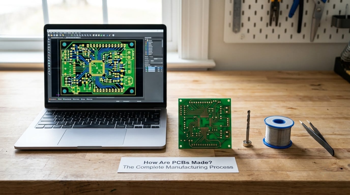
Here is the whole chain in the order it happens inside a fab.
- Design and preparation. An engineer draws the schematic, assigns footprints, routes copper and exports Gerber files plus drill data.
- Imaging and etching. Light transfers the artwork onto a photoresist layer, and chemical or laser etching strips away the copper that should not be there.
- Layering and drilling. Inner layers are stacked with prepreg and pressed, then a CNC machine drills vias and pads that are electroplated with copper.
- Masking, finishing and testing. Solder mask and silkscreen go on, a surface finish protects the pads, and the board gets inspected and electrically tested.
Fabrication and assembly are different jobs. Everything above builds an empty board with copper on it; assembly is the separate stage where components are placed and soldered onto that board.
What Is a PCB and Why Is Manufacturing Important?
A printed circuit board is a flat panel of insulating material with conductive copper patterns on one or both faces. The copper traces replace the web of point-to-point wires a circuit would otherwise need, and the glass laminate holds the traces in a fixed shape so the same board comes out the same way every time.
That repeatability is the whole reason fabs exist. A hand-wired prototype might work on your bench and fall apart in someone else’s. A fabricated board arrives with the geometry, spacing and layer stack already locked in, which is what makes automated pick-and-place possible in the first place.
For anyone building electronics in a salty, wet environment, it also becomes a materials question. A board that works on a desk has to survive condensation, salt spray and thermal cycling before it goes near the water.
How Are PCBs Made From a Schematic?
Manufacturing starts before anyone touches copper. The schematic defines the circuit, the layout places those parts physically, and the netlist is what links the two together.
- Schematic capture. Components are drawn with correct pin numbers and values, and the tool runs an electrical rules check for unconnected pins and power net conflicts.
- Footprint assignment. Every symbol gets a land pattern matching the real package, down to pad numbers and pin one marker.
- Stack-up and board outline. You choose layer count, copper weight, material and dimensions. A four-layer board is the common compromise between complexity and cost for anything with a radio on it.
- Routing. Traces, ground planes and vias are placed. Differential pairs need matched length, and anything that crosses between layers needs a via.
- Design rule checks. The software flags traces that are too thin, gaps too narrow, or pads sitting too close to the board edge.
- Gerber export. Each layer becomes a separate Gerber file, with a drill file and an outline file for the router. This package is the only thing the fab sees.
Most forums I have read on this topic share the same lesson: mistakes that survive to the CAM stage are the expensive ones. A wrong footprint or a missing ground via costs a redesign cycle no matter how good the board otherwise is.
How Are PCBs Made Using Different Manufacturing Methods?
Not every board is built the same way. What changes is layer count, whether the substrate bends, and how the copper gets onto it.
Single-sided boards have copper on one face only. They are cheap, easy to inspect and fine for simple relay or LED circuits.
Double-sided boards put copper on both faces and connect them with plated through-holes. This is the default for prototypes and small control boards.
Multilayer boards press inner signal and plane layers between prepreg and outer layers. Four layers is the sweet spot most designers land on, because a dedicated ground plane does more for signal behaviour than any amount of careful routing on two layers.
Rigid-flex boards combine stiff FR-4 sections with flexible polyimide sections in one board, so a sensor can sit on a moving part without a cable. They cost more because the process stacks and etches different materials.
HDI builds use laser-drilled microvias stacked in layers, allowing far denser fanouts for fine-pitch parts such as BGAs.
Then there is the route itself. Subtractive etching removes copper from a sheet. Additive processes build copper up chemically and are the basis for most advanced boards, since laser microvias and sequential lamination are additive steps. Panelization groups many boards onto one sheet, with mouse-bites or V-scores separating them after processing.
What Happens During PCB Fabrication?
1. CAM review and panelization
A CAM engineer loads your Gerbers, checks them against the fab’s process and builds the panel. DFM feedback at this point can still be fixed cheaply, which is why good fabs offer it before the order is released.
2. Material preparation and cutting
Copper-clad laminate is cut to size and its edges ground smooth. FR-4, a glass-reinforced epoxy, covers most needs; polyimide, PTFE or metal-core materials are chosen for flexibility, high temperature or thermal conductivity.
3. Imaging the artwork
A cleaned laminate gets a thin layer of photoresist, which is dried and exposed to UV light through the Gerber artwork. Where the light hits, the resist hardens and protects the copper underneath. Direct imaging replaced film photoplotters in most fabs because it is sharper and needs no film handling.
4. Etching away unwanted copper
Exposed copper is removed with ferric chloride or an ammoniacal solution, leaving only the traces and pads defined by the design. Laser etching is used where a cleaner edge or very fine geometry matters. The resist strip comes next.
5. Drilling and via formation
A CNC drill machine cuts component holes, mounting holes and vias. Drills are tiny, measured in fractions of a millimetre, and the tool has to be replaced often as it wears. Through-holes and vias need plating; blind and buried vias are created by filling the hole on one side with dielectric before plating.
6. Copper plating
Electroplating grows copper inside the drilled holes and on the remaining surface, creating barrel walls that connect the layers and tie the outer copper to the pads.
7. Lamination for multilayer boards
For a four-layer or higher board, each copper layer is imaged, etched and inspected before being stacked with sheets of prepreg. The stack goes into a heated press that bonds it into a single solid laminate under controlled temperature and pressure.
8. Outer layer imaging and etch
After lamination, the outer copper layers go through the same imaging and etching cycle, and the drilled holes are cleaned out. On high-density boards, via tenting or via filling keeps solder and plating chemistry out of the barrels.
9. Solder mask and silkscreen
Liquid solder mask is screened or printed over the board and UV-cured, leaving pads open. Every board gets a mask, and its colour is a convenient way to tell layers apart on a stack-up. The silkscreen then prints reference designators, polarity marks and outlines onto the mask.
10. Surface finish, routing and inspection
The exposed copper gets plated with the finish you chose: HASL for low cost, ENIG for fine pitch, OSP for good solderability. The board is then routed or scribed to size, given a surface treatment for moisture resistance, and checked. Any defect that fails inspection is scrap, which is why the checks matter so much.
How Are PCBs Made With Surface Mount and Through-Hole Parts?
Assembly is where the empty board becomes a working device, and there are two dominant methods.
Surface mount is handled by a pick-and-place machine, which feeds components from tape and reels onto the pads and then runs the board through a reflow oven. The solder paste printed before placement melts and pulls each component into place as the board moves through a controlled temperature profile. It is fast, repeatable and handles parts far smaller than a grain of rice.
Through-hole parts push their leads through plated holes in the board, which makes them mechanically strong and easy for a human to inspect or rework. Bulk through-hole boards can go through a wave solder machine, where a wave of molten solder passes over the underside. Hand soldering with an iron is still the norm for prototypes.
Mixed assemblies are normal in practice: a control board with a fine-pitch microcontroller in the middle, through-hole headers, terminals and mounting hardware around the edge. SMD keeps the board small; through-hole keeps the important connectors serviceable.
How Are PCBs Made for Marine Electronics?
Boat instruments and ocean robotics add a set of requirements that a dry indoor prototype never faces.
Salt and standing moisture attack copper traces, pads and connectors from the outside in. Conformal coating, applied after assembly and cured into a thin film over the board, blocks the path water and salt would otherwise take. It is not a seal against immersion, but it slows corrosion dramatically. Pressurised housings and breathable membranes do the rest of the work.
Connector choice matters as much as coating. Marine-rated connectors are gold-plated, sealed against the environment, and chosen for a mating cycle count rather than a price list.
Temperature swings on a hull are the other stressor. Repeated heating and cooling expands a bimetallic stack of FR-4 and copper, so asymmetric builds can warp, and a cracked via or a lifted pad follows. Balancing copper across layers and specifying a material with a suitable glass transition temperature reduces it.
Testing for this kind of build is not just a bench check. Boards go through humidity soak, thermal cycling and vibration testing, and a marine supplier should be able to say plainly what they have run and on which batches.
How Do Manufacturers Check PCB Quality?
Inspection happens at several points because a defect caught early is cheaper than a defect caught at the end of a full order.
Design rule and CAM checks run before fabrication, comparing the design against the fab’s rules for minimum trace width and spacing, minimum annular ring around a drilled hole, and board edge clearance.
Electrical testing comes after plating. A flying probe tester touches every net to check for opens and shorts; a fixture bed with gold-plated probes runs the same test faster and far cheaper on volume orders. Impedance-controlled boards ship with test coupons so the fab can verify trace geometry on a material sample.
AOI inspects the finished outer layers for missing traces, shorts and surface defects using cameras. X-ray inspection looks under solder mask at solder joints on BGA and QFN parts, where a joint can look perfect and still be a cold solder. X-ray also confirms that vias really are plated.
Assembly adds its own checks: AOI on the placed board, X-ray on the joints, then a functional test that exercises the design in firmware. The paperwork matters too. A certificate of conformance, RoHS and REACH declarations, and an IPC class statement tell you what standard the run was built to. IPC Class 2 suits most consumer and instrumentation work; Class 3 is for high-reliability builds with tighter controls on things like coplanarity and defect limits.
Frequently Asked Questions
How do PCBs work?
A PCB works by carrying current along copper traces whose shapes are set during design. The traces connect component pads in a fixed circuit, so signals and power move along predictable paths. Ground and power planes carry return currents across the whole surface of a layer, which is why layer count affects electrical behaviour as much as trace layout.
What are the steps involved in PCB manufacturing?
The main steps are design and Gerber preparation, material cutting, photoresist imaging, etching, drilling, copper plating, lamination for multilayer boards, outer layer imaging, solder mask, silkscreen, surface finish, routing and electrical testing. Assembly is separate: pick-and-place, reflow soldering or through-hole soldering, then inspection and functional test.
Are PCBs made of plastic?
Usually not, though the material family is similar. Most boards use FR-4, a glass-fibre cloth soaked in epoxy resin and covered in copper foil. Flexible sections use polyimide film, high-frequency boards use PTFE, and some LED and power boards use aluminium or copper as a metal core. The plastic impression comes from the resin, but the structural strength is the glass.
What is a Type 3 PCB?
Type 3 is an IPC-6012 classification for high-reliability boards, not a different manufacturing method. It allows more defects in cosmetic areas than Class 2 while tightening controls on functional ones, such as via fill, annular ring and hole tolerance. Aircraft, medical and satellite programs typically specify it, along with full inspection and test coverage.
Can you make PCBs at home?
You can, at low resolution. The usual home route is drawing artwork on laser printer paper, using that as a photographic mask for photoresist-coated copper board, and etching in ferric chloride, then drilling by hand. It works for single-sided hobby boards. Fine traces, multilayer builds, plated vias and anything that must survive outdoor or marine use need a real fab.
What is the difference between PCB fabrication and assembly?
Fabrication makes the empty board: copper, mask, silkscreen, finish and drilled holes. Assembly puts the components on it. Many suppliers offer both, so a single order can arrive as a tested, working assembly. Specifying them separately is normal when you are sourcing parts yourself or when a design changes after the boards are already built.
Conclusion
So how are PCBs made? A design is captured as artwork, transferred to a copper-clad laminate with light, reduced to the copper the circuit needs, drilled and plated so the layers connect, then sealed with mask and finish, inspected, tested and assembled. Every stage after the design step is chemistry, heat and precision machining working to a millimetre and a fraction.
If you are starting your first board, do three things. Build a correct schematic and footprint library before routing anything, run the design rule check and read the fab’s capability list with the CAM report open, and pick the manufacturer on layer count, material, finish, quantity and whether they will assemble it. For anything going near salt water, add conformal coating and a proper humidity and thermal cycling plan to the conversation before the order is placed.